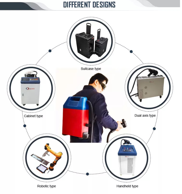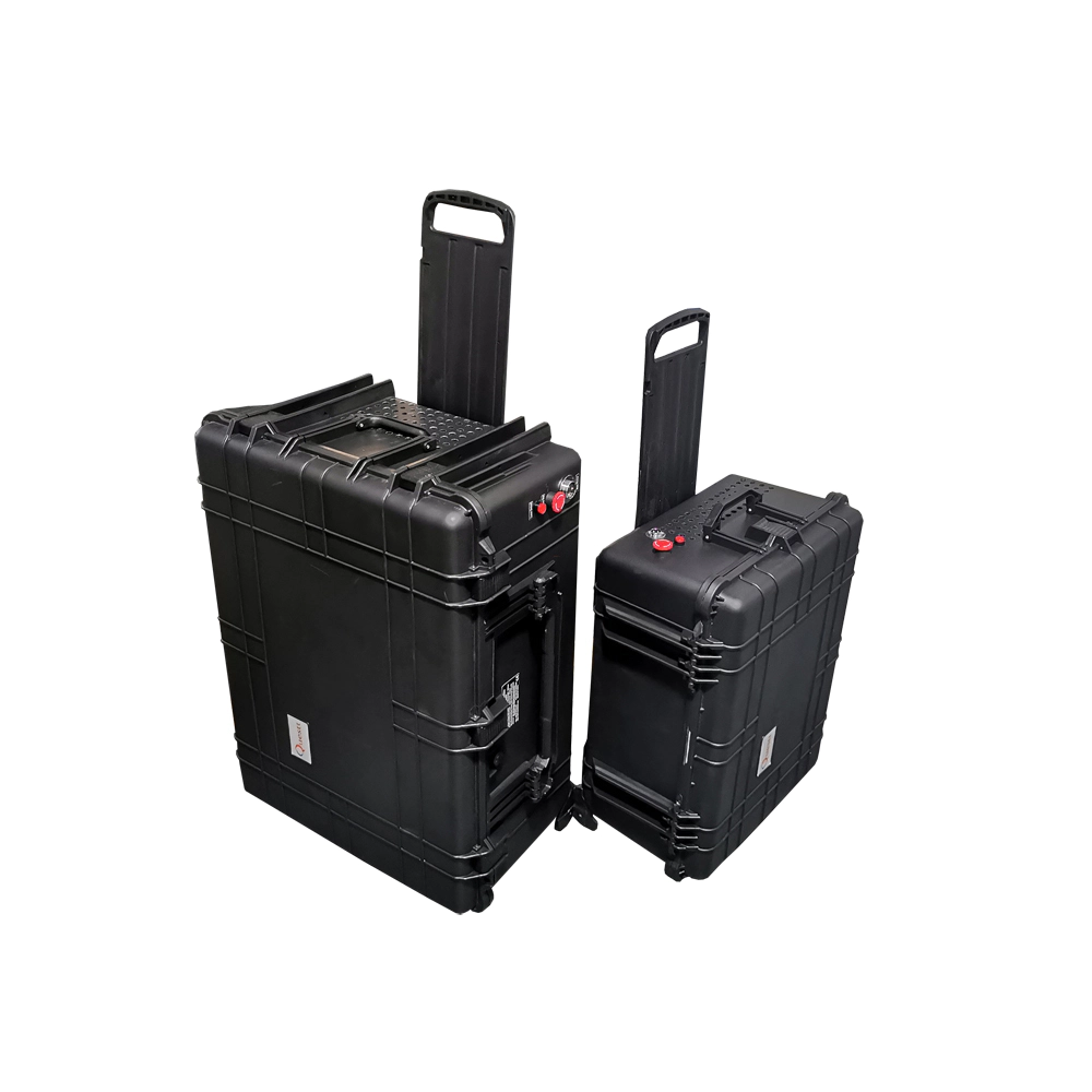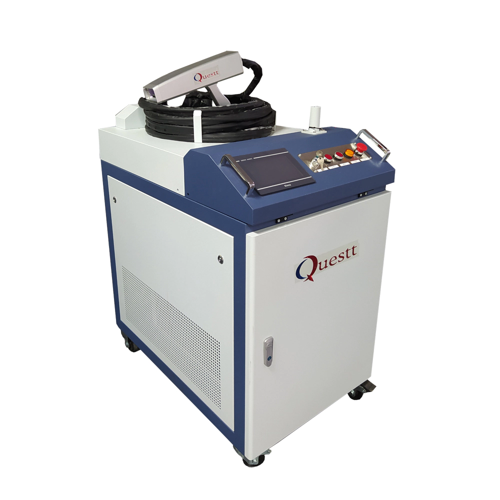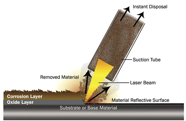

What are the advantages of laser cleaning compared to traditional cleaning?
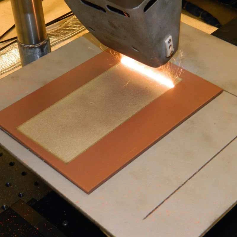
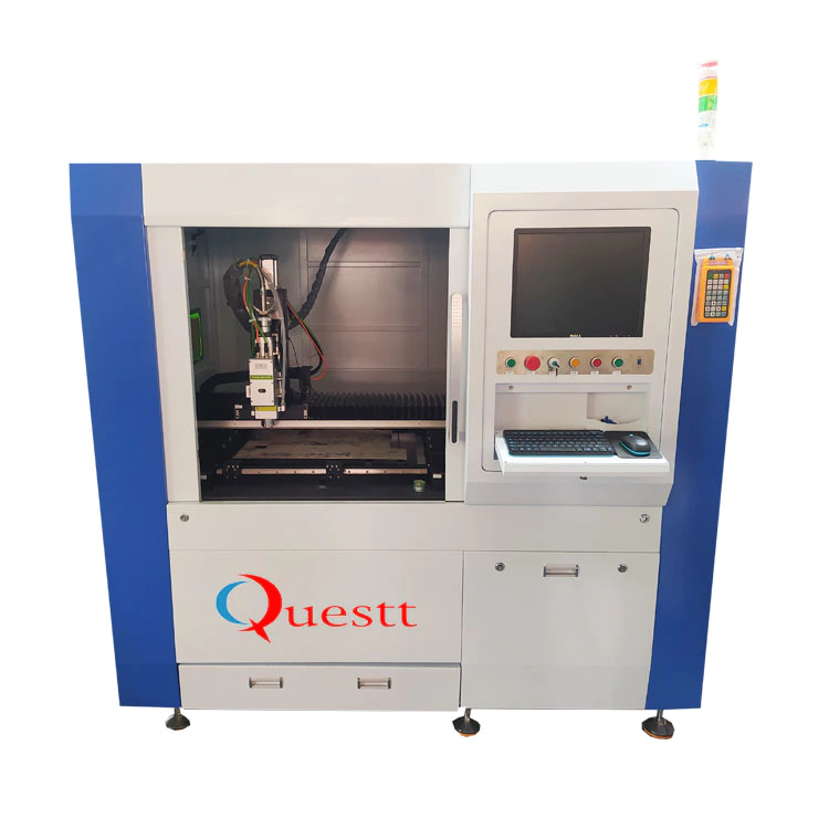
Double-sided PCBs With a Laser Cutter
by:QUESTT
2020-04-21
With a little practice, you can make a good double.
Get a double sided pcb by combining the laser cutting machine with chemical etching.
The basic idea is that the laser cutter blows up the spray-painted etching glue, and then the chemicals eat the exposed copper.
Once the copper disappears, the bottom plate can be cut again with a laser to pass through-holes.
No drilling required!
After some setup and practice you should get 8-
Mill traces/spaces and hundreds of holes in about 2 hours.
You can even cut internal wiring and odd boardshapes!
You will never want to do this, but if you want to do the same --
The prototype of the new design is perfect.
I love the process because I don\'t need to wait 2 weeks to get back from fab so I can actively design and try new ideas.
If you are in a research lab or store, you will find the materials effortlessly, but you should also be able to find everything you need in hardware stores and pharmacies.
This structure will take a step. by-
By making a two-step process
Side plates, pay special attention to the use of software to produce a good laser path, as well as some clever tricks to help keep the top and bottom of the plate well aligned.
Leave me a message if you have feedback or new ideas! The steps are:(1)
PCB inventory with paint coating (2)
Laser cutting spring-
Formal alignment fixture (3)
Optimize board layout for manufacturing (4)
Generate a vector diagram for the tool (5)
Etching off black paint with laser on both sides (6)
Chemical etching of exposed copper (7)
Laser cutting-
Holes on the exposed plate (8)
Tips and tricks for welding the DIY boundary materials you need: cutting PCB blanks using laser (try www. inventables. com)Spray paint (
McMaster #7719T9)
Acrylic 6 \"x 6\" between 1/8 and 1/4 thick \"(3 mm -6 mm)
For the manufacture of jig drill press or rotary tool with small drill bits (
Optional but helpful for alignment)
Gloves, gogglesNon-
Hydrogen peroxide, metal plates, measuring devices and tools (3%)
Hydrochloric acid (30-
37%, also called muratic acid)
You also need some software access: PCB design, export to a format that the graphics program can read (
I export to EPS with Eagle)
Vector graphics program for editing art.
I\'m using Adobe Illustrator.
Short notes on safety and environment: If you can use a laser cutter, you should be familiar with the dangers in it.
However, these instructions also guide you through copper chloride etching that may not be familiar.
The chemicals used are dangerous.
Hydrochloric acid can burn your skin and make you blind and produce toxic smoke.
Hydrogen peroxide reacts with a large number of substances, heavy metals (copper)are poisonous.
Always working outside (
Or in a chemical fume hood)
Wearing gloves and goggles
Make sure you have adult supervision if you are under 40 years old.
Finally, don\'t put your etching waste in the drain
It can do harm to people and the environment.
Store it safely in a labeled container and handle it properly by contacting a hazardous waste disposal agency in your area.
Existing technology: many have previously documented the parts of the process in detail.
I like it very much: you should have a look at these. Alright.
Let\'s start!
First of all, you need to get some PCB blanks.
I found FR1 (
Stock of paper and resin base)
Laser cutting is more reliable (
No toxic smoke)
Fr4 than traditional fiberglass.
If you want to pass-
Wiring holes or plate edges.
You can buy FR1 copper
Wearing two sheetsand double-
Next, you need to paint a one-sided flavor on the stock on both sides with paint.
Good luck to you, Rustoleum flat black (
McMaster #7719T9).
Choose the thinnest coating, you can get a reliable coating and make an error on one side where the paint is insufficient (
You can touch it.
Ups with Sharpie mark later).
Thin paint is important because when you blow up the paint with a laser, its film will be re-deposited.
The thinner the paint layer you spray away, the less things you relocate.
Keep the nozzle at least 18 inch from the board to obtain a coating with uniform light. (
By the way, I tried some other spray coating
An acrylic base, an Epoxy Base
Find something that does not leave an anti-etching fog.
But the black apartment seems to work best. )
It takes about 15 minutes at the top.
Side paint to dry before flipping the plate.
Try to keep the paint on the back-
One side of the same thickness, otherwise the two sides of the plate may be etched at different rates.
The paint is messy, so either do it where no one cares, or do it where you won\'t get caught.
I usually do a batch of about 10 boards at a time and keep them.
Be careful not to scratch when you store paint. (
But if you do, you can get back in touch later. )
Repeatable alignment for double
Because you will put the PCB in the laser cutter three times. (
The pattern at the top, the pattern at the bottom, then pass through again
Holes after chemical etching. )
If the pattern on the top and bottom is not aligned then your pass
Holes will not line up either;
This is sub-optimal. (
The hole that does not pass through anything is not a hole but a dent. )
I found a simple laser. cut spring-
The form fixture makes alignment easier.
The model provided works for 2 \"x3\" boards, but you can use it for larger inventory. (
I have included the DXF and Adobe Illustrator files-
Please feel free to modify them. )1/8\" (3 mm)
Acrylic is good for this but you can go all the way up to 1/4 \"(6 mm)
If that\'s what you have
Careful attention to the alignment of the fixture ensures that the top of the PCB is consistent with the coordinate system of the tool. (1)
Cut the profile from the acrylic material (
You need a square with 6 \"x 6)
, Then place the cutter in the upper left corner of the cutter bed block. (2)
Now cut the interior pattern.
Align the upper left corner of the pattern [0. 50\",0. 50\"]
In the coordinates of the laser
This will keep the upper left corner edge of the PCB placed in [1. 00\",1. 00\"]. (3)
Mark the text annotation at the top of the fixture with a grating. (. . . if desired.
These are included only in the Illustrator version of the file. )
Now you should be able to bend the spring in the fixture and lean the plate against the top left corner. Don\'t over-do it.
The acrylic fiber is very hard so you can shoot it downflexing.
However, the additional design of the 2 \"x3\" plates includes blocks to prevent this.
Also, do not try to install the board on the fixture as it is on the tool honeycomb bed --
You will scrape off the paint on the underside of the board as it will scratch onto the metal.
Creating a good PCB layout is a big topic and different boards have different requirements, but the DIY process adds some limitations.
Here are some tips for making your motherboard easy to build :(1)
Conservative design traces and spaces.
You may be able to get traces of 8/8 mil, but you need to look closely at the etching.
So make as many traces as possible, can, and willspaced.
In the sample design shown in the figure, the smallest trace is.
016 \"wide and causes 32-
TQFP package is available in the center. (2)
Remember, through-
Holes are not plated.
So if an assembly has traces that cause it on each side of the board, you need to weld it on each side.
For some simple components, but other components-
Especially the connector with plastic flange, flush with the circuit board
This is impossible.
Therefore, only the components on the side of the circuit board that can be welded are tracked. (
You can also be creative.
For example, pins in many 0.
1 \"the head can slide over the plastic cover.
Climbing up the body cloth can give you the space to weld, and then you can slide the body cloth back. )
This sample plate is designed to weld connectors only on the top (red)side. (3)
Make your vias big and rare.
Because through
The holes are not plated, you need to insert a wire in each hole and weld it on both sides. (
If you go through another part, make sure you weld via first! )
So, make your vias big enough for the wires you use.
The 25 mil holes on the 50 mil pads are both convenient and sturdy. (4)
Your circuit board does not have a soldering mask, so it is harder to weld than a commercial PCB.
Therefore, through the pads, especially the top-, conservative running trajectory
Side pads that need to be welded around the assembly.
It is worthwhile to think carefully about the order in which the components are installed to make sure that you can get the iron in all the places you need it. (5)
Add a few extra holes (
Or large unconnected vias)
In unused areas
These are very useful for checking alignment. (6)
Your board will not have the legend of screen printing.
Usually, you can have a good time if you print the design on a nearby piece of paper, but it can be confusing if your design is dense, repetitive or complex.
I usually add some copper features that are not connected as markers.
For example, in designing a small copper is 32-in the upper right corner-
TQFP package is available in the center. (7)
Once you have a design that you like, you can export your art.
However, for holes, unlike the traditional process of generating a hole file, you actually need an image of the hole.
For example, in Eagle, you can generate it by selecting run ULP from the File menu. . .
\"And select drillaid. ulp. (Set the center-hole size to 0. )
This produces all the images.
Hole of 116 layer. (8)
To output several files (
Plate profile, top copper, bottom copper and holes)
In a format that the graphics program can view.
Eagle can generate the EPS file and the laserPCB that comes with it.
Set the cam file to automatically extract the appropriate layer.
Select from the File menu: \"CAM processor. . .
Then select File> open> job to open the provided laserPCB \".
Cam \"and click process job to generate the file.
Now that you have obtained images of copper and holes for your board, you need to import them into your graphics programprocessing.
I have written these instructions for Adobe Illustrator, but you should be able to do something similar in other vector graphics programs.
The goal of this process is to convert the art into a continuous path, outline the outline for the laser tracking, and offset the path to take into account the beam width of the laser.
Why not use the laser directly to grating all the paint except the copper trace?
Whenever the laser blows up the paint, it creates a fine mist that refixes the paint (
Even in the clear area)
Anti-etching.
To solve this problem, we remove as little paint as possible (
So less fog)
Passed many times.
When we chemical etching, it is also more effective to use this \"isolated etching\" method because there are fewer copper to dissolve. (1)
Open all EPS files in Illustrator and copy and paste their contents into a separate layer of a document. (Using [Ctrl]-
\"Paste in front\" will make sure the layers are aligned. )
Make sure all plate profiles are aligned so that the layers with holes will remain aligned with the copper traces.
Now you should set separate layers for the plate profile, top copper, bottom copper, and holes. (
The CAM processor outputs separate files for the top and bottom holes.
Savvy readers will realize that as holes, the holes will go through the top and bottom layers, so the files should be the same.
Select one of them and use it! )(2)
Top copper, bottom copper, and hole layers perform Step 2a-2d:(2a)
Select tracking (
But not the board outline)
, And run the object> path> outline stroke to create the path outside each tracking segment. (2b)
Now set the tracking width.
001 \", the color of the trace is red, and the filling is not filled. (
This may vary depending on your tool settings-
Select the tracking attribute that generates the vector cut. )(2c)
Select all tracking (
But not the board outline).
Now, in the Pathfinder tray, run \"Unite\" to merge overlapping paths to create a continuous profile for each copper track. This will fill-in any ringed-in structures.
It\'s not common to have these, but if so, you need to copy them into another layer before running this command.
It will also remove the holes in the center of the copper trace layer pad, but it doesn\'t matter because we will put them back from the \"holes\" layer. (2d)
Now let\'s illustrate the width of the laser.
This is usually the case with our laser cutting.
Width after etching
You will feel this after making a few boards.
Select track and run the object> path> offset path.
For offset values, enter half the width of the laser cut (
Our laser point is
\"Wide, so we enter.
004 \"this value may be a bit difficult to predict because it depends on the laser power and also because the etching process will make the cut a little wider.
You will understand after making a few boards).
Increase this value if you want a wider tracking.
If you do this for the hole layer, please enter-. 004”.
This will make the interior of the hole smaller to take into account the width of the laser point.
Illustrator will not remove the old path, so you will need to cut and paste the new offset path to the new layer. (
The new offset path will be the only one selected after running the offset path, so only [Ctrl]-
X cut them, make a new layer, and [Ctrl]-F paste them. )(3)
If you want to laser cut the outline of the board or any internal wiring, remember that in order for the laser to pass through the board, you need to etching the copper first, so you need the etching marks on both sides.
Put them on a separate layer so you will remember to do so. (4)
Set the plate profile to a different color that does not produce a cut.
You don\'t want to remove it because it usually helps to align the art with the tool coordinate system. (5)
We are separating traces from the background copper, but leave the background copper in place.
Therefore, if we accidentally leave multiple marks on the background copper, it will produce a connection that we do not want.
You can break the copper background by drawing a few etching lines on the copper background, thus giving yourself a safe space.
This makes it less likely that you accidentally short more than one signal to a copper background, and it will be much easier to diagnose if you do, because you only need to check the boundaries of a small piece of copper.
Just don\'t accidentally draw a cut on any of your marks!
Now we\'re starting to light one!
Before you do the whole board, you will want to do some testing etches to determine how much power to use. A few hints:(a)
Use the tightest focal spot lens you can find and make sure you focus precisely on the top surface of the board.
The wide beam point will make the separation between your traces too wide (
Your marks are narrower). (b)
Use enough power to pass through the paint, but too much power will make the cut wider. (c)
Passed many times.
I found 4 great ones.
The subsequent pass will not expand the cutting range, but will remove the paint mist for re-cutting
Deposited in the traces removed.
After 4 passes, the exposed copper should be bright and shiny with no obvious black residue.
Once you have the settings you like, you can start etching the board. (1)
Place the plate in the fixture, and the fixture rests on the block.
You can prevent the metal bed honeycomb from scratching the board by placing a spare acrylic sheet under the board and fixture. (
You won\'t burn through the boards at this step, so you won\'t be hurt. )
This should put the top left corner of the board [1. 00\",1. 00\"]
In the coordinates of the laser
When you move the red aiming beam [1. 00\", 1. 00\"]
You should see it scattered down the corner of the PCB. (2)
Align your art so that the top left corner of the chessboard outline is located [1. 00\",1. 00\"]. (3)
There are now laser etching marks and holes;
Do it 4 times in order.
We need to etching the paint on the hole profile to clear the copper on the hole profile so that we can laser cut the penetration holes in later steps. (4)
Remove the plate from the fixture.
The fixture helps to align, but if the PCB stock size is not exactly 2 \"x 3\", it still causes dislocation when you flip the board to do the bottom.
To check this, please select a pass
Etching the holes or holes outlined and drilling the penetration holes to the other side using a drilling machine. (
The most common passholes are . 040\". )
Using the extra unattached holes you add to your design makes this easier because you don\'t have to worry about missing and accidentally drilling through the liner.
It may be difficult to give the drill center on the small pad.
If your hole is a little small
The center does not sweat.
Just drill holes as a reference to make sure the pattern is incorrect
Both sides agreed. (5)
Now turn over the board and put it in the fixture.
I found out-
A better alignment than flipping to the left
Yes, maybe because the size of the 2 \"plate is more accurate.
Remember, whether in Illustrator or in the tool driver, also reflect your art about this axis to illustrate the fact that you flipped the board! (6)
Pick the path through-
The hole you drill in order to align, put it on a separate layer and try etching the hole.
If your alignment is off and the etching is not concentric with the drilling, please add some offsets in the coordinates of the laser and try again until you get a good match. (7)
Now etching the bottom
Use the same process as the top track to draw the side track and hole profile. (
Again, make 4 passes. )
Now that you \'ve exposed some copper on both sides of the board, it\'s time to etching it off.
You can use the storebought ferric-
A favorite chlorine etching agent near you
E-shop, but these things are disgusting and I have good experience in copper chloride process.
Because both processes use acid and heavy metals, they are potentially dangerous for you and the environment: wear gloves and goggles and do so outdoors or in a chemical fume hood.
Don\'t pour chemicals in the sewers.
Store them in non
Metal-enclosed containers and take them to hazardous waste disposal facilities.
You need: gloves, goggles and old clothes (or a lab coat)
3% hydrogen peroxide (
Standard for drug stores)
37% hydrochloric acid (
Also known as Muratic acid, Pool)Paint thinner (
Pine or acetone)Non-metallic (
Glass or plastic)
Container and measuring cup. (
Etching will dissolve the metal.
This is the point. )
Plastic tongs, toothpicks, pipettes or feathers. Paper towels.
Before you start, double check the board to make sure all the areas you don\'t want to etching are still covered with black paint.
If you have some missing insurance (
The honeycomb bed of the laser cutting machine sometimes scraped off the paint)
Clean up with a marker. (0)
Wear gloves and goggles! Safety first.
Optional helmet. (1)
Pour 2 parts of hydrogen peroxide into nonmetallic (
Plastic or glass! )container. About a half-cup (or 100 mL)
Is a reasonable starting amount. (2)
Slowly add 1 piece of HCl (
About 1/4 cups (50 ml).
This will emit some heat.
Do it slowly and add acid to the water instead of the other way around to avoid splashing. (3)
Place the plate at the etching and moisten both sides. (4)
Gently shake the container to move the fluid and the board.
The use of plastic tools or toothpicks can help locate the plate.
The pipettes or droppers are very useful for spewing bubbles formed.
Feathers can do the same. (5)
After a few minutes, when the copper is dissolved, you will notice that the etching begins to turn green.
Turn the plate every few minutes and continue to stir. (6)
After a few minutes, pull the plate out, soak it in tap water, and check the marks under a magnifying glass or microscope.
You should see some areas where the red copper has been etched to expose the tan or gray substrate of the underlying layer.
Put it back in the etching to make sure both sides are wet. (7)
Check the blackboard every few minutes to see if it\'s done.
Error on the lower sideetching.
There are usually some stubborn spots that resist etching;
Cleaning up these things with a blade is much easier than trying to ensure the continuity of a bunch of moths --
Traces of eatingetched. (8)
Once you are satisfied with the etching, rinse immediately in tap water for 30 seconds, then remove all paint immediately with paint thinners and paper towels.
If you do not peel off the paint immediately, the acid absorbed into the paint will continue to slowly etching the underlying copper and you will endetched. (9)
You can usually get several uses from your etchant, but it needs to be charged once it is deep emerald color.
Please remember to dispose of waste in a safe and eco-friendly manner.
If you\'re going to store it, make sure it\'s in a solid non-
Metal container, clearly labeled, marked as poison.
Now, you have etched the copper around you --
The laser cutting machine can pass through the exposed FR1 substrate.
Put the plate back in the elastic fixture and align the image of the hole layer again with the coordinate system of the tool.
Again, it is often helpful to check your alignment and laser power by trying to cut a test hole.
Since the exposed copper reflects the laser to a large extent, you can tolerate moderate dislocation at this step --
Only the exposed FR1 will be cut off.
However, you can get enough charring to crush the base plate under the pad, so you want to set the laser power to let it go through the board at one pass, but the characters on the edge of the hole do not exceed the necessary characters.
Once you are satisfied with your test holes, continue to cut them.
You can also cut any wiring or circuit board-
As long as you have etched the copper from above, you have made the profile shape.
If you are aligned well, you should get clean holes on the entire board and do not need to re-align
Cut holes from the back of the plate.
If you have some misplacement then sometimes the second pass (
Maybe from behind.
Side of the board)
The cut-outs on both sides can be helped deep enough to meet the demand, but it is possible to burn the substrate that supports some pads.
The hole plug itself may not fall off cleanly.
Poke with solid
The core wire should pop up right away.
Laser cutting holes are very helpful for plates with a large number of holes that require a lot of work done manually on a drilling machine, or many-
Several pin misplacement can result in hard-to-insert fixed parts.
This is also great for strange people.
You may not have a bit of a hole in size, or wiring to cut the board into a new shape.
Now that you have finished making the board, some tips and tricks for actually filling and soldering the board.
Because these need to be welded at the top and bottom, and there is no welding mask, they are a little harder than the commercial plate, but not impossible. (1)
Visibility is the name of the game: you can see anything.
As long as you can see, even a small pitch pad is easy to weld with a fine tip.
So it takes some time to set up the magnifying glass (on a holder)
Or find an old anatomical microscope. (2)
Tin paste and reflux furnace can be used (or hot plate)
For fine surface mounting parts, but I found this to be more troublesome than its value.
You can really weld tiny parts easily with good visibility.
But if you do try to return, consider laser cutting the mai la solder paste template --
They work very well. (3)
Before welding the assembly, check the tracking continuity and isolation with a multimeter.
It is much easier to separate some incomplete etched areas using a razor blade (
Or a little tin cream to clean up a Wikipedia. etched trace)
The way there were components before. (4)
Consider coloring the pads before you try to weld them.
Using an iron to melt a little bit of solder on each pad is very fast, and if the pad already has solder moistened, it will make it easier to weld the assembly.
This is especially true for surface mount pads. (5)
Before filling any other components, weld the holes first.
Use the stripped solid core line, weld it on both sides, and then use the Clippers to clamp it flat. (6)
Be careful not to lift the pad when inserting the lead.
If you cut a misplaced hole, then you may lift the edge of the copper from the burnt substrate. Just go easy.
When this happens, the pads fold instead of breaking, so you can usually bend them into shape with tweezers or Wells
Put your nails. (7)
Be strategic about the part you place first.
I usually start at the center of the board and work towards such a high place outside (
The TO220 package is fierce in big yuan)
Don\'t block the soldering iron. (8)
There are some welding Wick for easy cleaning of unexpected bridges.
However, it is usually only necessary to run a hot iron head in the groove between the marks to clear the bridge. (9)
These boards are indeed for prototyping, but consider coating them if you need some solid material (
After all parts are welded)
Spray with hard insulating epoxy.
Custom message
Related Products